

A continuous roller printing method that can pick up and transfer more than 75,000 semiconductor devices with a size of less than one micrometer in a single roll has been developed by researchers. The new technique opens the door to producing massive arrays of optical parts and may be utilized to produce micro-LED screens quickly.
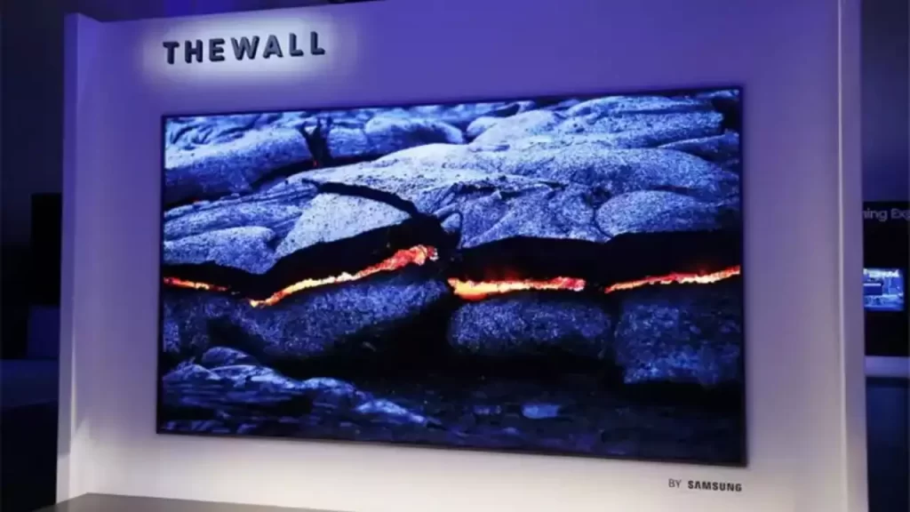
Micro-LED screen technology is quite intriguing because it can provide very accurate color rendering with high speed and resolution while consuming minimal power. These displays may be used in a variety of forms, such as smartphone screens, augmented reality and virtual reality headsets, and enormous displays that are several meters in diameter.
The difficulties of integrating millions of tiny LEDs, some of which are as small as a grain of fine sand, onto an electronic control backplane are significant, especially for bigger micro-LED screens.
In the journal Optical Materials Express, the researchers say their innovative roller technique can match the specified device layout with a precision of less than 1 micron. Additionally, the arrangement is affordable and straightforward enough to be built in areas with limited resources.
Other types of devices, such as silicon and printed electronics such as transistors, sensors, and antennas for flexible and wearable electronics, smart packaging, and radio-frequency identification tags, might also be produced using this printing technique.
Additionally, it could be helpful for biological uses including tissue engineering, medication delivery systems, biosensors, and photovoltaics.
The extensive device transfer
Nowadays, multi-layer, finely detailed semiconductor thin films are deposited onto semiconductor substrates utilizing growth processes, which are then used to fabricate semiconductor devices on wafers.
The applications of the devices are limited by compatibility concerns between these thin film structures and the kinds of substrates acceptable for this deposition.
To enhance the performance and scaling of electronic systems used in applications like displays and on-chip photonics, where the goal is to combine various materials that manipulate light on a very small scale, Margariti said, “We wanted to improve the transfer of large numbers of semiconductor devices from one substrate to another.”
“It is critical to use methods that can transfer these devices efficiently, accurately, and with few errors to be used for large-scale manufacturing.”
The new method begins with a collection of microscopic objects that are slackly fastened to the growing medium. It is very effective for large-scale production since the printing process is continuous and may be utilized to print several devices at once.
Extremely precise printing
Gallium nitride on silicon (GaN/Si) semiconductor structures were used to test the novel method. It was made easier to prepare the devices as suspended structures that the roller could pick up by utilizing silicon substrates, as GaN is the predominant semiconductor technology utilized for micro-LED displays.
With a spatial accuracy below a micron and no major rotational errors, they were able to transfer more than 99% of the devices in an array of more than 76,000 unique pieces.
The next goal of the researchers is to scale up the number of devices that may be transferred simultaneously while still increasing the precision of the printing process.
Additionally, they want to see if the technology can be used to print to certain areas of the receiving platform and how well it works when many device types are combined into one receiving platform.

READ ALSO – Facebook Parent Meta Makes Its AI ChatGPT Competitor LLaMA 2 Public
The next iteration of Meta’s AI large language model, known as LLaMA 2, will be made available for free for study and commercial usage, according to the company’s CEO, Mark Zuckerberg, who made the announcement on Tuesday.
